
The Technical Anatomy of a Digital Image: From Photons to Forensic Evidence
Introduction
Digital photography represents the convergence of physics, electronics, and algorithmic computation. It transforms the analog world of light into discrete, structured data that can be interpreted, manipulated, and authenticated. This paper explores the end-to-end mechanics of digital imaging—from photon interaction at the sensor to color reconstruction and forensic verification. Through an in-depth examination of image sensor technology, noise modeling, demosaicing algorithms, and authentication tools, we aim to provide a comprehensive understanding of the digital image as both a visual and evidentiary medium.
1. Image Sensor Fundamentals
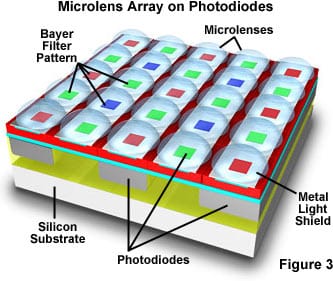
At the heart of a digital camera lies the image sensor, typically a CMOS (Complementary Metal-Oxide-Semiconductor) or, less commonly, a CCD (Charge-Coupled Device). These integrated circuits function as a two-dimensional array of photodiodes—semiconductor devices that convert photons into electrical charges using the photoelectric effect.
The performance of an image sensor is characterized by several parameters: spatial resolution, quantum efficiency (QE), dynamic range, signal-to-noise ratio (SNR), and readout speed. CMOS sensors dominate the market due to their lower power consumption, faster readout, and on-chip functionality such as analog-to-digital converters and gain amplifiers. CCD sensors, although largely obsolete in consumer imaging, are still used in specialized scientific applications for their superior uniformity and low-noise performance.
Each photodiode in the sensor corresponds to a pixel and is responsible for gathering light from a small region of the image. When photons hit the photodiode's depletion region, they excite electrons across the silicon bandgap, creating electron-hole pairs. The electrons are collected in a potential well, and the total charge accumulated over the exposure time is proportional to the light intensity incident on that pixel.
Said in another way...
Each photodiode on a digital camera sensor is one pixel in the final image. Its job is to measure the amount of light hitting it during an exposure.
When light (made up of photons) hits the silicon inside a photodiode, it transfers energy to the material. If the photon has enough energy, it knocks an electron loose. This is called photoelectric conversion.
The knocked-loose electron and the “hole” it leaves behind form what’s called an electron-hole pair. The photodiode is designed to collect those free electrons in a tiny storage area called a potential well—think of it like a bucket under a faucet.
The longer the exposure or the brighter the light, the more electrons accumulate in that well. After the exposure ends, the camera reads out the total charge—how many electrons were in that bucket. This number is proportional to the amount of light that hit that pixel.
To summarize:
- Light hits a pixel.
- The energy frees electrons in the silicon.
- The freed electrons are stored.
- More light = more electrons.
- The camera measures how many electrons were stored to figure out how bright that pixel was.
The construction of the photodiode and its relationship to the sensor's overall architecture plays a critical role in determining the efficiency and fidelity of light-to-charge conversion. Several design parameters affect this performance:
Pixel pitch refers to the center-to-center distance between adjacent photodiodes. Smaller pixel pitches allow higher resolution but can reduce the amount of light each pixel captures, potentially lowering signal-to-noise ratio (SNR), particularly in low-light conditions.
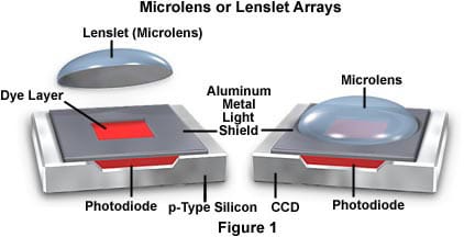
Fill factor describes the proportion of each pixel's surface area that is photosensitive. A high fill factor means more of the pixel's surface is used to detect light, improving sensitivity. Modern sensors enhance fill factor through microlenses that direct more light into the active photodiode area.
Pinned Photodiodes (PPDs) are a specialized photodiode structure designed to reduce noise and improve charge transfer efficiency. By 'pinning' the surface potential, PPDs suppress dark current (thermal noise) and allow for more complete and controlled transfer of photo-generated charge to the readout circuitry.
Charge Transfer Efficiency (CTE) is another critical aspect, especially in CCDs but relevant in CMOS as well. Inefficient charge transfer can introduce image lag or noise, particularly in fast-readout or high-speed burst modes.
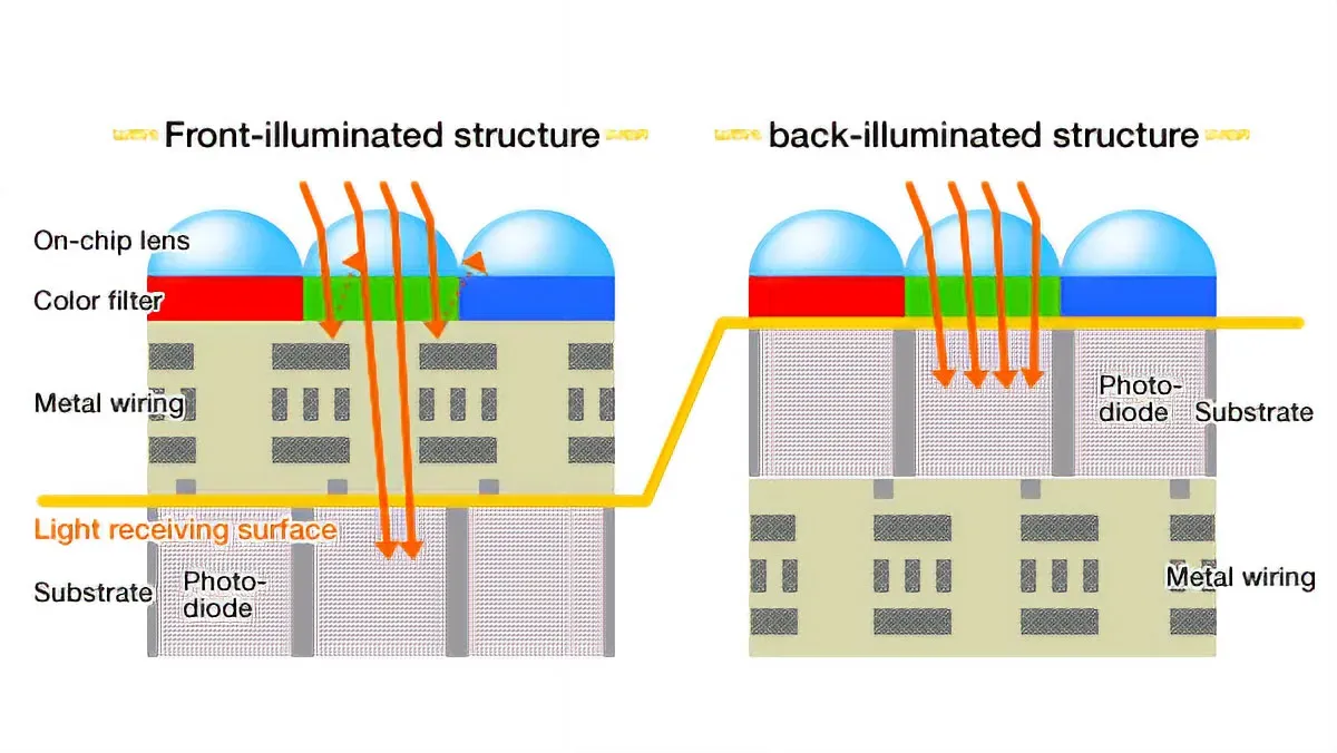
To further optimize sensitivity, particularly in small-pixel designs, modern sensors increasingly use Backside-Illuminated (BSI) architecture. In BSI sensors, the metal wiring and transistors that traditionally sit above the photodiodes (in front-side-illuminated sensors) are moved to the rear of the substrate. This restructuring removes optical obstructions, allowing more photons to reach the active layer of the photodiode. The result is improved quantum efficiency, better low-light performance, and the ability to maintain high image quality even with reduced pixel size.
Advanced CMOS fabrication also integrates analog-to-digital converters, noise suppression circuits, and gain amplifiers at the pixel or column level, enabling faster, more accurate signal processing.
Through this combination of photonic sensitivity, semiconductor design, and advanced fabrication techniques, the image sensor serves as the entry point of the digital imaging pipeline—capturing the analog shadow of a scene and converting it into quantifiable electronic data for further processing.
1.1 Photon-to-Electron Conversion
Each photodiode forms a p-n junction within the silicon substrate. When photons enter the depletion region of this junction, they generate electron-hole pairs. The electrons are collected in a potential well, and the amount of charge accumulated is proportional to the intensity of incoming light. Quantum efficiency (QE) measures how effectively photons are converted into electrons.
1.2 Color Filter Array (CFA)
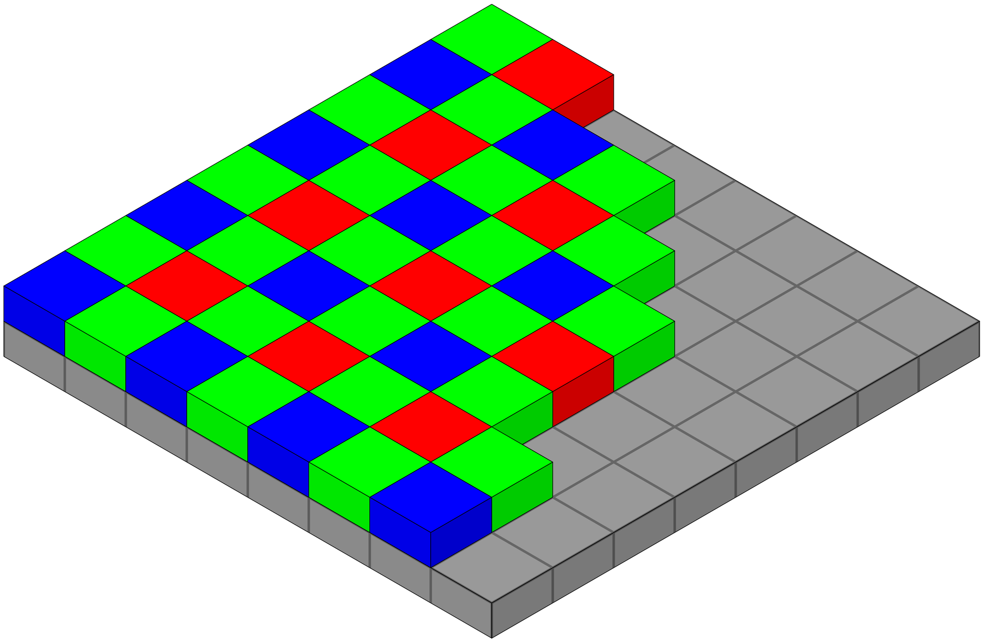
Because photodiodes do not inherently detect color, a Color Filter Array (CFA) is used. The most prevalent is the Bayer filter, a 2x2 grid pattern with two green, one red, and one blue filter. This configuration leverages the human eye's heightened sensitivity to green light.
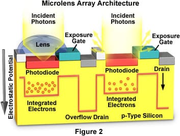
1.3 Microlenses and Fill Factor
Microlenses are placed above each pixel to direct light into the photodiode’s active area, increasing the fill factor—the ratio of light-sensitive to total pixel area. This maximizes light efficiency and reduces loss due to internal reflection or wiring obstructions.
2. Signal Readout and Digitization
After exposure, the electrical charge from each pixel is read, amplified, and digitized.
2.1 Charge-to-Voltage Conversion
In APS (Active Pixel Sensor) CMOS designs, each pixel includes a charge amplifier. This converts the collected charge into a voltage signal, which is then routed for digitization.
2.2 Analog Gain and ISO
In digital photography, ISO represents the amplification level applied to the sensor’s output before the signal is digitized. This amplification occurs after light has been converted into an electrical charge by each photodiode but before it is read and converted into a digital value by the analog-to-digital converter (ADC).
Increasing ISO does not make the sensor more sensitive to light—it boosts the voltage signal generated from the collected electrons. This makes the resulting image appear brighter, which is useful in low-light conditions. However, amplification affects both the signal (desired image information) and the noise (unwanted variation).
At low ISO settings, the signal is stronger relative to noise, producing clean images. As ISO increases, read noise, thermal noise, and shot noise are all amplified alongside the signal, which can lead to graininess and a reduction in image quality—especially in the shadows and flat tones.
Modern sensors include dual or multi-stage analog gain circuits, allowing the camera to switch between gain modes that are optimized for either low-light performance or high dynamic range.
2.3 Analog-to-Digital Converter (ADC)
The ADC translates the voltage into a digital value, typically 12 to 16 bits per channel. This process introduces quantization noise, especially significant in low-light environments with a weak signal.
3. Demosaicing: Reconstructing Color via Interpolation
As discussed, each pixel on a sensor using a Bayer Color Filter Array (CFA) only captures one color channel: red, green, or blue. This means two-thirds of the color data at every pixel must be interpolated—that is, estimated—based on neighboring pixel values. The process of demosaicing reconstructs a full RGB value at every pixel location.
3.1 Bilinear Interpolation: A Foundational Algorithm
One of the simplest and earliest demosaicing techniques is bilinear interpolation. Though crude by modern standards, it’s instructive for understanding the fundamental challenges in color reconstruction.
Let’s define the Bayer CFA in a 3x3 pattern:
G R G
B G B
G R G
In this simplified layout:
- G = Green
- R = Red
- B = Blue
Suppose we want to estimate the full RGB value at a green pixel. Let’s walk through a concrete example of estimating R, G, and B at a pixel that is green.
3.2 Example: Estimating RGB at a Green Pixel
Assume the green pixel is at position (1,1) (zero-indexed), surrounded by values:
(0,0) G=120   (0,1) R=100   (0,2) G=130
(1,0) B=90    (1,1) G=125   (1,2) B=95
(2,0) G=135   (2,1) R=110   (2,2) G=140
The green value at (1,1) is already known: G = 125
To estimate the missing R and B, we use bilinear interpolation:
- Estimate R at (1,1) as the average of the red values at horizontal/vertical neighbors:
- R at (0,1) = 100
- R at (2,1) = 110
- Average = (100 + 110) / 2 = 105
- Estimate B at (1,1) as the average of the blue values at horizontal/vertical neighbors:
- B at (1,0) = 90
- B at (1,2) = 95
- Average = (90 + 95) / 2 = 92.5 → round to 93
Interpolated RGB at (1,1):
R = 105
G = 125
B = 93
This process is repeated for every pixel, using a pattern-specific strategy depending on whether the pixel is originally red, green, or blue.
3.3 Why Bilinear Falls Short
While fast and easy to implement, bilinear interpolation tends to blur edges and produce color artifacts:
- Zipper effect: jagged edges where color transitions are misestimated
- Color moiré: false color patterns in fine detail, especially in fabrics or screens
- Loss of sharpness: due to averaging across boundaries
3.4 Toward Smarter Interpolation: Edge-Aware Methods
To mitigate these problems, edge-aware interpolation techniques like Gradient-Corrected Linear Interpolation (GLCI) or Adaptive Homogeneity-Directed (AHD) demosaicing adapt the interpolation direction based on image structure.
For example, in GLCI, the algorithm checks the intensity gradients in horizontal and vertical directions:
- If there’s a strong vertical edge, interpolate color values along the edge rather than across it, preserving sharpness and reducing color bleeding.
This is conceptually:
if abs(G(x-1, y) - G(x+1, y)) < abs(G(x, y-1) - G(x, y+1)):
    # interpolate horizontally
else:
    # interpolate vertically
These more advanced methods produce better detail retention and fewer artifacts but come at a higher computational cost.
Conclusion: Why Interpolation Matters
Interpolation is not just a technical detail—it’s a visual bottleneck. The fidelity of demosaicing determines the accuracy of color, sharpness, and perceived quality of a digital image. While bilinear interpolation shows the basics, modern algorithms rely on dynamic, edge-aware processing that balances signal integrity with computational feasibility.
4. Noise: Sources and Characteristics
Noise is an unavoidable component of digital imaging, stemming from multiple sources:
4.1 Shot Noise and the Nature of Discrete Photonic Events
At the heart of digital imaging lies a surprisingly profound concept: the behavior of light is fundamentally discrete, not continuous. Rather than arriving as a smooth stream, light reaches a camera sensor in individual, quantized packets of energy known as photons. Each of these photons, when absorbed by a photodiode in the sensor, may trigger the release of a single electron via the photoelectric effect. This one-to-one relationship—one photon leading to one photo-generated electron—illustrates how image formation begins with a series of discrete events.
Because these photon arrivals occur randomly over time, even under constant lighting, they introduce a statistical variation known as shot noise. This noise is not caused by flaws in the sensor, but rather emerges from the quantum nature of light itself. Shot noise follows a Poisson distribution, where the variance (or expected level of fluctuation) is equal to the average number of photon events. This means the amount of noise increases with the brightness of the scene, but crucially, it increases more slowly—specifically, in proportion to the square root of the signal level. For instance, if a pixel receives 10,000 photons, the shot noise is roughly √10,000 = 100, resulting in a signal-to-noise ratio (SNR) of 100:1.
This statistical behavior places a fundamental limit on image quality, especially in low-light conditions where fewer photons are captured. With a small signal, shot noise becomes a more prominent part of the total data. As such, many characteristics of an image—like clarity, dynamic range, and tonal smoothness—are directly influenced by how many discrete photon events occur and how well the sensor handles them.
Understanding shot noise as a product of discrete photonic events bridges the technical with the philosophical. It reminds us that a digital image is not just a visual impression, but a record of countless individual interactions between light and matter—measurable, statistical echoes of the real world rendered pixel by pixel.
4.2 Thermal Noise
Thermal noise, also known as dark current noise, is generated when heat energy within the image sensor causes electrons to become excited and break free—even when no light is present. This process occurs because at any non-zero temperature, atoms in the silicon lattice vibrate. Occasionally, this thermal energy is enough to excite an electron into the conduction band, mimicking the effect of a photon.
The result is that some pixels collect false signal—electrons that were not triggered by light but rather by heat. This can lead to elevated base levels in the image (called dark current) and introduce grainy patterns or specks, especially in the shadow areas or during long exposures, where the sensor has more time to accumulate thermally generated charge.
Thermal noise increases exponentially with temperature, making it especially problematic in warm environments or with passively cooled consumer sensors. To mitigate it, professional and scientific cameras often use active sensor cooling, such as Peltier coolers or even liquid nitrogen systems in astrophotography, to maintain a stable and low sensor temperature.
In modern CMOS sensors, design optimizations like pinned photodiodes (PPDs), optimized fabrication materials, and correlated double sampling (CDS) also help reduce the effects of thermal noise. Still, cooling remains one of the most effective ways to suppress thermally induced signal errors and preserve image quality, particularly in long-exposure or high-dynamic-range imaging.
4.3 Read Noise
Read noise refers to the electronic noise introduced during the process of converting and extracting the stored charge from each pixel into a usable digital signal. Even in total darkness, a camera sensor may report small fluctuations in pixel values—not because light was detected, but because noise was introduced during the readout process.
This type of noise comes from several sources:
- Amplifier noise: After photons are converted to electrons and collected in a potential well, the resulting charge is extremely small. Before digitization, this signal must be amplified. However, amplifiers inherently introduce random electrical noise due to thermal fluctuations in the transistors and resistive elements—this is known as Johnson-Nyquist noise or flicker noise.
- Charge-to-voltage conversion variability: As the analog charge is converted into a voltage, slight differences in the characteristics of each pixel’s circuitry can introduce variation. This results in pixel-to-pixel inconsistencies, especially in low-light conditions where the signal is weak.
- Analog-to-Digital Converter (ADC) noise: Once the signal is amplified, it is digitized by the ADC. Any imperfections in timing, voltage reference levels, or resolution limitations in the ADC can introduce further inaccuracies into the final digital value.
Unlike shot noise, which is a fundamental property of light and scales with signal strength, read noise is a fixed baseline—a constant level of uncertainty added to every pixel, regardless of how much light is present. In very low-light or short-exposure scenarios, read noise can dominate the image and obscure faint details.
Advancements in sensor design have significantly reduced read noise in modern CMOS sensors. Techniques like correlated double sampling (CDS), column-parallel ADCs, and low-noise amplifier designs help minimize its impact, allowing for cleaner images even in near-dark conditions.
4.4 Fixed Pattern Noise (FPN)
Fixed Pattern Noise (FPN) is a type of image noise that appears as a consistent, repeating pattern across an image—often visible as vertical or horizontal streaks, banding, or faint textures. Unlike shot noise or read noise, which are random, FPN is systematic and occurs because of pixel-to-pixel variations in the sensor’s electrical characteristics.
These variations are introduced during the manufacturing process. Each pixel may have slight differences in:
- Dark current (baseline leakage of electrons)
- Gain response (how strongly the pixel amplifies charge)
- Offset voltage (baseline electrical level)
- Analog circuitry performance (due to minute structural mismatches)
The result is that, even when a sensor is uniformly illuminated or completely covered (e.g. in a dark frame), some pixels consistently report values that are slightly too high or too low compared to their neighbors. This creates a fixed pattern that is “burned in” to the sensor’s behavior and does not change frame to frame.
Fortunately, because FPN is consistent, it can be characterized and corrected. Modern cameras perform on-chip or in-software calibration using dark frames (images taken with the shutter closed) or flat-field frames (uniformly lit scenes). These reference images help identify and subtract out the fixed noise pattern, reducing its visibility in the final output.
Advanced correction techniques in post-processing software and in-camera signal pipelines now make FPN virtually invisible under normal use. However, it can still become apparent in long exposures, extreme low-light scenarios, or when pushing shadow detail in post.
5. Image Processing Pipeline
Following the initial demosaicing stage, the raw sensor data undergoes a series of processing steps designed to convert the linear, monochromatic signal into a visually accurate and usable digital image. Each stage in this pipeline plays a critical role in shaping the final output and can influence both the perceptual qualities of the image and its validity in forensic or scientific contexts.
- White Balance Adjustment: Since the sensor captures different wavelengths through color filters, white balance corrects for the color temperature of the light source by scaling the red, green, and blue channels. This ensures neutral tones appear consistent under varying lighting conditions.
- Color Space Transformation: The sensor’s native color values are mapped into standard color spaces such as sRGBor AdobeRGB. This transformation allows for consistent color representation across displays and devices, and is essential for archival or comparative work.
- Gamma Correction: The linear luminance data from the sensor is remapped to a non-linear gamma curve that better matches human visual perception. This step compresses midtones and expands highlights and shadows to preserve detail and create a more natural-looking image.
- Noise Reduction: Both chromatic and luminance noise are suppressed through a combination of spatial filtering(which smooths local pixel neighborhoods) and frequency domain techniques (which target noise patterns without significantly degrading detail). Effective noise reduction improves image clarity, but excessive application may obscure or distort fine features.
- Sharpening: To enhance edge definition and counteract the softening effects of demosaicing and noise reduction, sharpening algorithms apply convolution kernels—typically unsharp masking or high-pass filters—to emphasize contrast at image boundaries.
- Compression: Finally, the image is encoded into a chosen file format using either lossless (e.g., PNG, TIFF) or lossy (e.g., JPEG) compression. Compression affects file size and quality, with lossy formats potentially discarding subtle image data that may be relevant in forensic analysis.
Each of these steps alters the raw sensor data to produce a visually coherent image, but they also introduce transformations that may obscure or alter original signal characteristics. As such, the image processing pipeline must be carefully managed when images are intended for evidentiary use or scientific measurement, where fidelity to the original scene is paramount.
6. Forensic Image Authentication
While digital images undergo extensive transformation through demosaicing, color correction, noise filtering, and compression, they can still serve as valid evidence in forensic investigations—provided their integrity is preserved and their origin can be verified. Forensic image authentication focuses on evaluating whether an image is original, has been tampered with, or can be reliably attributed to a specific device. Below are the primary methods used in forensic contexts:
6.1 RAW File Integrity
RAW files are the most forensically valuable image format because they contain minimally processed data directly from the image sensor. These files include the raw mosaic of sensor values along with metadata about the sensor, lens, and shooting conditions. Since RAW files bypass most of the image processing pipeline, they are far less susceptible to manipulation. Forensic analysts can examine pixel-level patterns, sensor response curves, and embedded hash values or signatures (when supported by the camera). Validation of a RAW file’s integrity is often done by comparing embedded checksums or digital signatures to verify that no data has been altered.
6.2 Metadata Analysis
Every digital image file includes EXIF (Exchangeable Image File Format) metadata, which stores auxiliary information such as timestamp, GPS location, camera make and model, aperture, shutter speed, and ISO. This metadata can be cross-referenced with witness accounts, surveillance logs, or device records. Tools such as ExifTool, X-Ways Forensics, and PhotoME are commonly used to inspect, extract, and compare metadata. However, since metadata can be modified or forged, analysts often look for inconsistencies—such as improbable camera settings, mismatched timestamps, or missing tags that are normally present in a given device’s output.
6.3 Sensor Pattern Noise (PRNU)
Every digital image sensor exhibits unique manufacturing imperfections that lead to slight pixel-to-pixel variations in sensitivity. These variations form a reproducible pattern known as Photo Response Non-Uniformity (PRNU), which acts like a fingerprint for the sensor. By analyzing the PRNU pattern of an image and comparing it to a reference PRNU extracted from a known device, forensic experts can determine whether a photo was taken by that specific camera. This technique is particularly powerful in cases involving child exploitation, harassment, or surveillance, where image attribution to a suspect’s device is crucial. PRNU analysis is sensitive and requires statistical correlation techniques, often aided by software tools like Amped Authenticate, CameraForensics, or custom MATLAB-based pipelines.
6.4 Clone Detection and Tamper Analysis
In addition to source verification, forensic analysts must assess whether an image has been digitally manipulated. Common manipulations include cloning, splicing, object removal, or lighting alteration. Software such as Forensically, Amped Authenticate, and Izitru use algorithms to detect artifacts from these actions by examining patterns of JPEG compression blocks, inconsistencies in lighting and shadows, duplicate pixel patterns, and statistical anomalies in noise distribution. Techniques such as Error Level Analysis (ELA), JPEG quantization grid analysis, and light source triangulation can reveal signs of tampering that are invisible to the naked eye.
In forensic workflows, multiple techniques are often used in tandem to form a more comprehensive analysis. Proper chain-of-custody documentation, version tracking, and use of original media formats further enhance the evidentiary value of digital images in legal contexts.
Conclusion
Digital images are far more than mere visual impressions; they are intricate data constructs, born from a deep interplay between quantum physics, semiconductor engineering, and signal processing. At the core of every image lies a chain of discrete photonic events—individual photons striking silicon, generating electrons, and initiating a cascade of analog and digital transformations. From the construction of photodiodes and the precision of analog gain circuits to the probabilistic nature of shot noise and the subtle fingerprint of sensor imperfections, each layer contributes to the final image in measurable, meaningful ways.
This complex process does not merely serve aesthetic or practical ends—it also produces an evidentiary record that, under the right conditions, can withstand forensic scrutiny. Proper handling of RAW data, awareness of metadata integrity, and advanced authentication techniques such as PRNU matching and clone detection enable digital photographs to function as reliable artifacts in legal and investigative contexts. As such, a digital image is not just a picture—it is a structured, time-stamped, and device-specific document.
The ongoing evolution of sensor technology, computational photography, and image forensics continues to push the boundaries of what can be captured, interpreted, and proven. Whether in the hands of a photographer, a scientist, or an investigator, the digital image stands as both a product of light and logic—a carefully measured imprint of reality shaped by the physical limits of light and the creative possibilities of computation.
References:
